Working on the NXP FRDM-MCXA156 PAC: Day 1
published:
[!NOTE] I will be using a lot of Embedded systems Jargon in this blog post. So just in case I have added a definitions section at the bottom. Or you can click the footnotes next to some words to view its definition.
I recently got my hands on the NXP FRDM-MCXA156 board, courtesy of the Embedded Online Conference (EOC) pass. Naturally, my first step was to take it for a spin. Since I didn't wanna use Arduino for this (Who still uses Arduino nowadays), I selected Zephyr RTOS, since this board had out-of-the-box support for Zephyr RTOS. I used Zephyr to test the hardware and also learn Zephyr along the way.
Next, I wanted to try Embedded Rust of this board (obviously). But then I ran into a problem.
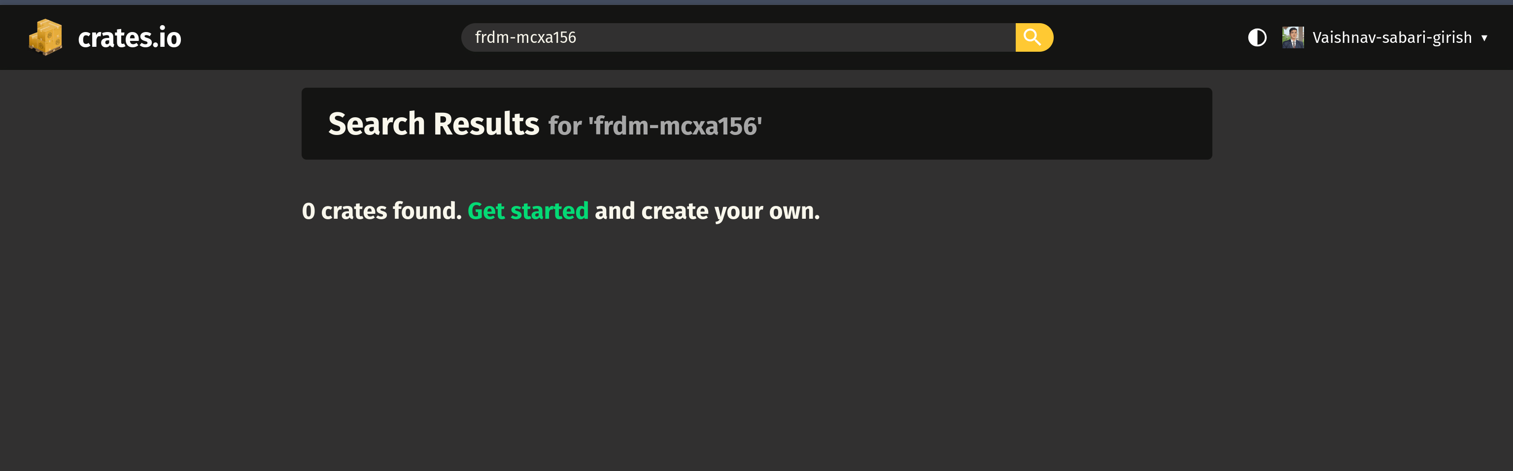
Where are all the crates for this board ?
Turns out that there are none. No HAL (Hardware Abstraction Layer), no BSP (Board Support Package). Not even a basic PAC (Peripheral Access Crate). If I wanted to run Rust on this Cortex-M33 board, I had to build it
Well luckily I could find a few materials to refer. For the starting point, I used Jacob Beningo's session on The Peripheral Access Crate as my primary reference. I tracked down NXP's SVD files, fired up svd2rust, and generated my very own frdm_mcxa156_pac (Magic!).
So the first step after the PAC was of-course testing it on the board. And the "Hello World!" equivalent of Embedded systems is basically blinking the on-board LED which I have done hundreds of times.
If that's the case, it must have worked right ?
If only it were that easy.

Getting a bare-metal microcontroller to blink an LED is easy enough. But doing it with a freshly generated, untested PAC means navigating clock trees, reset controllers, and bootrom quirks entirely from scratch.
So what did you do to make it work ?
So I am now in frdm_mcxa156_pac, I have documented everything I did.
For reference, here is the repository (Very vanilla repository, I am yet to add CI/CD and stuff).
Link: https://github.com/Vaishnav-Sabari-Girish/frdm_mcxa156_pac
The Hardware Context
So for starters here are the basic details
| Item | Detail |
|---|---|
| Board | NXP FRDM-MCXA156 |
| MCU | MCXA156 (Cortex-M33, 96 MHz FRO) |
| Green LED | GPIO3 pin 13 (active low) |
| Red LED | GPIO3 pin 12 (active low) |
| Blue LED | GPIO3 pin 0 (active low) |
| Debug probe | Onboard MCU-Link with J-Link firmware |
[!IMPORTANT] For debugging I am using the onboard MCU-Link flashed with the J-Link firmware
But why ? Isn't there a default one. CMSIS-DAP. Why not use that ?
So during initial testing, probe-rs was throwing intermittent DAP fault errors with the onboard firmware. Plus J-Link is faster and better as shown in the Zephyr Documentation itself
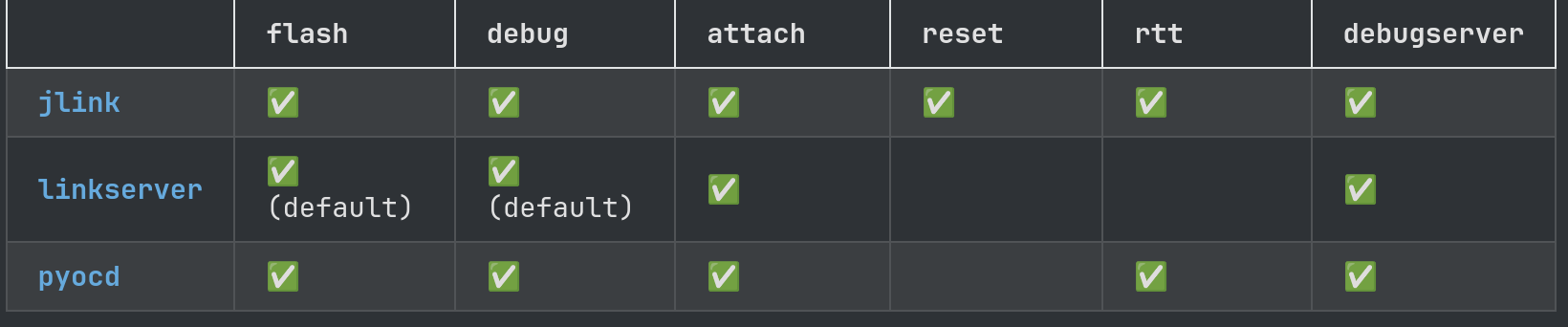
Now coming to the hurdles I faced.
Hurdle 1: The stubborn ROM bootloader
You know those moments when you make it all the way to the airport, only to realize you've forgotten your passport? That's essentially what happened here.
The first major roadblock had nothing to do with Rust or my PAC. The MCXA156 ROM was entering ISP (In-System Programming) mode instead of booting the application at 0x00000000. The vector table1 was perfectly valid, but the ROM requires a Boot Configuration Area2 (BCA) header that I had not yet included.
So how do you execute code when the bootloader refuses to jump to it ?
As a temporary workaround for early development, I have bypassed the ROM entirely. A runner script flash.sh loads the binary and explicitly sets the Program Counter3 (PC) to the reset vector
For context here is the script
#!/bin/bash
# Flash a binary to FRDM-MCXA156 via J-Link and bypass ROM
BIN="$1"
SCRIPT=$(mktemp)
cat > "$SCRIPT" <<FLASH_EOF
device MCXA156
si SWD
speed 1000
connect
r
h
loadfile $BIN
SetPC 0x800
g
qc
FLASH_EOF
JLinkExe -NoGui 1 -CommanderScript "$SCRIPT"
rm -f "$SCRIPT"
I configured the runner command in .cargo/config.toml to run this script instead of the default probe-rs download command. So now when I run cargo run --example blinky --release, it runs this script.
Hurdle 2: Write Reordering and Silent Failures
Nothing hits harder than failure..... Or so I thought.
What hits harder is failing and not knowing what the hell went wrong ?
So what went wrong ?
So after verifying the code execution, I moved on to configuring the peripherals using my working (Heh) PAC.
In the MCX series of microcontrollers, peripherals are gated and held in reset by default.
So, if I wanted to use GPIO3, I had to enable it's clock in the GLB_CC1 register, then release it from reset via the GLB_RST1 register.

Initially, my code looked logical: enable clock, release reset, configure pin.
Instead of blinking an LED, the CPU threw as precise fault at the PORT3 pin control register (BFAR=0x400BF0B44, BFSR.PRECISERR=15, HFSR.FORCED=16)
I'm kinda lost. What do these errors mean ?
These specific errors signify a bus fault which occurs during invalid peripheral access.
The root cause was AHB7 bus write ordering. The ARM Cortex-M33 AHB bus can reorder write_volatile operations. The GLB_RST1_SET8 store was arriving at the MRCC9 peripheral before the GLB_CC1_SET10 store.
Because the clock must be active before the reset can be released, the hardware silently ignored my reset command. The peripheral remained in reset, and subsequent accesses triggered the bus fault.
So how did you fix it ?
Well, I basically inserted a Data Synchronization Barrier11 (cortex_m::asm::dsb()) between the clock-enable and reset-release. This guarantees strict write ordering.
The working Blinky in Rust (Finally !!)
With the bootloader bypassed and the hardware ordering respected, we can finally flash the damn thing.
Except that it uses a lot of unsafe (First iteration).
This is because it uses Peripherals::steal() which bypasses Rust's singleton guarantees and returns the raw Peripherals object itself. So, it had to be put inside an unsafe block.
Then the LED logic used another unsafe function write_volatile. This was unsafe because the compiler could not verify if the pointer being written to is valid.
Same for the GPIO init.
This was the code (First iteration of working blinky)
[!DANGER] Use this code at your own risk.
#![no_std]
#![no_main]

use core::ptr::write_volatile;
use cortex_m_rt::entry;
use embedded_hal::delay::DelayNs;
use panic_halt as _;

// MRCC0 base (0x4009_1000)
const MRCC0: *mut u32 = 0x4009_1000 as *mut u32;
const GLB_CC1_SET: usize = 0x54 / 4;
const GLB_RST1_SET: usize = 0x14 / 4;

// PORT3 / GPIO3
const PORT3: *mut u32 = 0x400B_F000 as *mut u32;
const PCR13: usize = 0xB4 / 4;
const GPIO3: *mut u32 = 0x4010_5000 as *mut u32;
const PDDR: usize = 0x54 / 4;
const PSOR: usize = 0x44 / 4;
const PCOR: usize = 0x48 / 4;

#[entry]
fn main() -> ! {
    // Set up the cycle-counting delay timer
    let cp = unsafe { cortex_m::Peripherals::steal() };
    let mut delay = cortex_m::delay::Delay::new(cp.SYST, 96_000_000);

    // --- GPIO init (unchanged) ---
    unsafe { write_volatile(MRCC0.add(GLB_CC1_SET), (1 << 10) | (1 << 23)); }
    cortex_m::asm::dsb();
    unsafe { write_volatile(MRCC0.add(GLB_RST1_SET), (1 << 10) | (1 << 23)); }
    unsafe { write_volatile(PORT3.add(PCR13), 0); }
    unsafe { write_volatile(GPIO3.add(PDDR), 1 << 13); }

    loop {
        unsafe { write_volatile(GPIO3.add(PCOR), 1 << 13); } // LED ON
        delay.delay_ms(500_u32);

        unsafe { write_volatile(GPIO3.add(PSOR), 1 << 13); } // LED OFF
        delay.delay_ms(500_u32);
    }
}
Then how is it type-safe if it has so many
unsafe blocks
To make it type-safe and remove all the unsafe blocks, it was a one-line change to the Cargo.toml file.
I needed to add the critical-section-single-core feature to the cortex-m crate.
cortex-m = { version = "0.7.7", features = ["critical-section-single-core"] }This allowed me to access the type-safe PAC definitions for the peripherals.
This is the final iteration (For now).
#![no_std]
#![no_main]

use cortex_m_rt::entry;
use panic_halt as _;

#[entry]
fn main() -> ! {
    let p = frdm_mcxa156_pac::Peripherals::take().unwrap();

    // ---- Enable clocks ----
    p.mrcc0.mrcc_glb_cc1().modify(|_, w| {
        w.port3().enabled();
        w.gpio3().enabled();
        w
    });

    // DSB: guarantee clock enable completes before reset release
    cortex_m::asm::dsb();

    // ---- Release from reset ----
    p.mrcc0.mrcc_glb_rst1().modify(|_, w| {
        w.port3().enabled();
        w.gpio3().enabled();
        w
    });

    // ---- Pin mux: PORT3 pin 13 = ALT0 (GPIO) ----
    p.port3.pcr13().modify(|_, w| {
        w.mux().mux00();
        w
    });

    // ---- Data direction: pin 13 = output ----
    p.gpio3.pddr().modify(|_, w| {
        w.pdd13().pdd1();
        w
    });

    loop {
        // LED ON (active low: clear → 0 → LED conducts)
        p.gpio3.pcor().write(|w| w.ptco13().ptco1());
        cortex_m::asm::delay(96_000_000 / 2);

        // LED OFF
        p.gpio3.psor().write(|w| w.ptso13().ptso1());
        cortex_m::asm::delay(96_000_000 / 2);
    }
}
This iteration uses the type-safe Peripherals::take() which outputs an Option<Peripherals> instead of the raw Peripherals object.
Key Takeaways from Day 1
- Clocks, Resets and Barriers: Releasing a peripheral from reset must happen after enabling it's clock. Do not trust the bus to maintain this order - enforce it with a DSB Barrier.
- DAP12 Writes vs CPU Writes: Debugger (DAP) writes often appear to work flawlessly because the debugger inserts implicit barriers. Do not assume your code will behave identically without explicit synchronization.
- Read the Fault Registers: Checking
CFSR,HFSRandBFARimmediately pinpointed the exact bus fault address (0x400BF0B4), turning hours of blind guesswork into a targeted bug hunt. - Trust the minimal test: When bring-up stalls due to an issue, write the magic value (
0xDEADBEEF) to RAM and spin forever. It is the fastest way to confirm the CPU is actually executing your code before diagnosing peripheral issues.
Are the closure based register API's worth the verbosity
Absolutely. The PAC is always Zero-cost safety. Once you understand the hardware state, the typed modify and write accessors abstract away the bit-math dangers while compiling down to the exact same volatile memory writes.
[!NOTE] This was a very long blog with a lot of code. Thank you for reading till the end.
Result
Definitions
Vector Table: An array of memory addresses at the beginning of flash memory (usually starting at 0x00000000) that points to the interrupt handlers, the initial stack pointer, and the Reset Handler (where code execution begins).
Boot Configuration Area (BCA): A specific data structure stored in flash memory that NXP microcontrollers use to configure ROM bootloader behaviour upon startup, such as jumping directly to the application or enabling specific debug interfaces.
Program Counter (PC): A core CPU register that holds the memory address of the next instruction the processor needs to execute.
Bus Fault Address Register (BFAR): A Cortex-M system register that holds the exact memory address that triggered a precise bus fault.
Bus Fault Status Register - Precise Error (BFSR.PRECISERR): A hardware flag indicating that a data bus error occurred and the exact address that caused it has been successfully captured in the BFAR.
HardFault Status Register - Forced (HFSR.FORCED): A flag indicating that a configurable fault was escalated into a HardFault, usually because the specific fault handler was not enabled or another fault occurred while trying to handle it.
Advanced High Performance Bus (AHB): A high-performance internal bus protocol defined by ARM's AMBA specification, used for connecting the Cortex-M CPU to high-speed memory and peripherals.
GLB_RST1_SET: A specific hardware register on the MCXA156 where writing a 1 sets the corresponding bit in the Global Reset Control 1 register, effectively releasing a peripheral from it's reset state.
Multi-Rate Clock Controller (MRCC): NXP's peripheral module responsible for managing clock generation, distribution, and reset controls for the various sub-systems and peripherals on the board.
GLB_CC1_SET: A hardware register where writing a 1 sets the corresponding bit in the Global Clock Control 1 register, actively supplying a clock signal to a specific peripheral.
Data Synchronization Barrier (DSB): An ARM hardware instruction that enforces strict memory access ordering. It stalls the CPU pipeline until all pending memory operations (such as our write_volatile to the clock enable register) have officially completed on the physical bus, ensuring that subsequent instructions (like the reset release) do not execute prematurely.
Debug Access Port (DAP): Access Port): A hardware interface that allows external debuggers (like J-Link or MCU-Link) to directly access the microcontroller's internal memory bus and CPU registers without requiring the CPU to execute code